RAITH EBPG 5000 Plus

Electron beam lithography   /   RAITH

Contacts :   CAMBRIL   Edmond     /   LE GRATIET   Luc

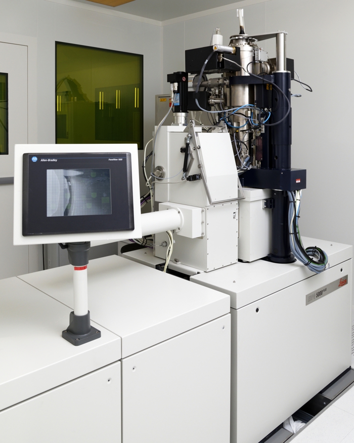
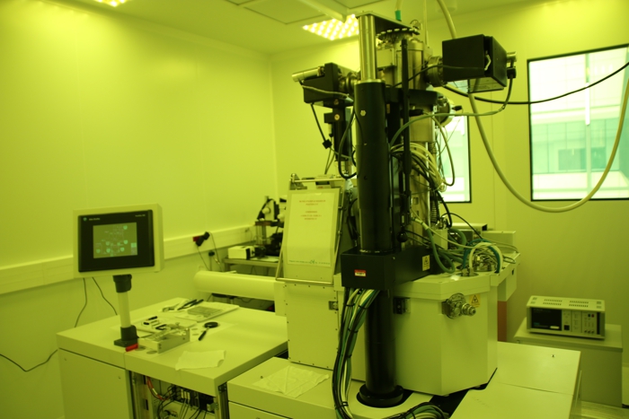
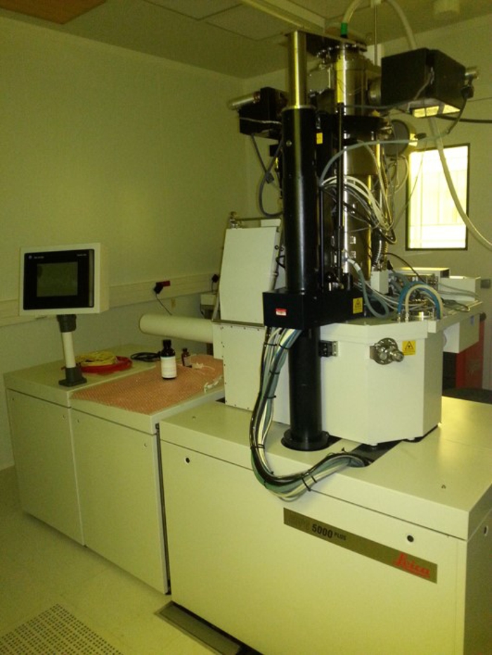
Raith EBPG 5000+ e-beam lithography tool is in operation since 2003. It has been set-up in a dedicated cleanroom of class 10 (ISO 4) with high precision temperature control at 21 ± 0.1° C. This stability in temperature is a prerequisite for the minimization of thermal drift in the electron optics, and thus, for the excellent performance of the system. The EBPG5000+ is a high performance nanolithography system used to pattern large areas by high-resolution electron beam lithography. It is a vector-scan direct write tool with a Gaussian shaped beam which operate up to 100 keV acceleration voltage with an exposure 125 MHz pattern generator. This instrument has substrate holders to handle samples of 10x10 mm² up to 4" wafers.

  • Space
    EBPG_5000_plus
  • Space
    EBPG5000
  • Space
    EBPG5000 +

Caractéristiques

  • Emitter   :   Field effect gun
  • Energy   :   100 keV
  • Frequency   :   125 MHz
  • Current   :   130 pA to 200 nA
  • Resolution   :   sub 20 nm
  • Positioning accuracy   :   0.6 nm
  • Writing field   :   160x160µm² to 1040x1040µm²
  • Substrates   :   1 cm square to 4 inches wafer
  • Spot size   :   5-6 nm at 5 nA
Expertises

Dense network in HSQ

Realisation of different network in 300nm HSQ resist on III-V materials. The minimum pitch and linewidth is below 100nm. The chessboard network is based on 200nm square

  • Space
  • Space

Contacts : Luc Le Gratiet, luc.le-gratiet@c2n.upsaclay.fr.

Combining raster and concentric writing strategy

By combining raster (longitudinal) and concentric writing, we can acheived very dense photonic crystal in GaAs. The resist is HSQ (180nm thick). The photonic crystal, after etching, is made of holes (diameter 130nm) with a smallest gap (20nm).

  • Space
  • Space
  • Space

Contacts : Edmond Cambril, edmond.cambril@c2n.upsaclay.fr

Tailoring ebeam lithography

Using GenIsys BEAMER for tailoring the lithography by modulating the dose. Fresnel Lens in PMMA

  • Space
  • Space

Contacts : Edmond Cambril, edmond.cambril@c2n.upsaclay.fr

Applications

Hybrid nanolaser diode

Realisation of an hybrid indium phospine-on -silicon nano laser diode, by combining 9 level lithography. The realization of the device implies tailoring the writing strategy in order to combine very low current and high current wrinting and the subsequent etching step.

  • Space
  • Space

Contacts : Fabrice Raineri fabrice.raineri@c2n.upsaclay.fr